Vlsi Schematic Design Principles Of Vlsi Design
4 bits multiplier design in electric vlsi with vhdl built layout Vlsi projects for mtech What is layout in vlsi
Design Projects in VLSI Systems | Stanford Online
My final project for vlsi: a 4-bit synchronous counter in 250nm cmos Vlsi: steps involved in vlsi design Introduction to vlsi system design
Vlsi cadence layout schematic full fiverr screen
Vlsi process ece principles advanced slides jimp intro unm c1 eduIntroduction to vlsi Vlsi design – sanjay vidhyadharanKlmh vlsi physical design from graph partitioning.
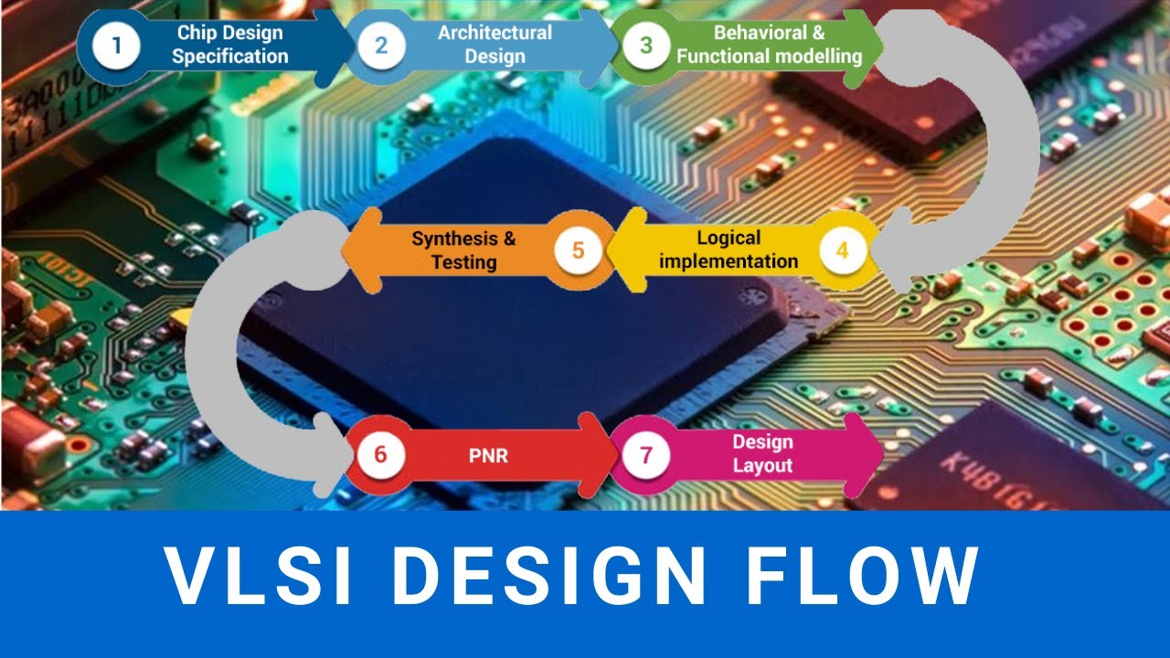
Principles of vlsi designVlsi design flow vlsi4freshers Vlsi course full form flow chip eligibility duration details fee career courses aimingVlsi diagrams nmos daigram jce.

Vlsi logic process testing fabrication functional principles
Vlsi flow basicsDiagram stick layout path euler vlsi part Cmos inverter 3dVlsi system introduction.
Vlsi basics: vlsi design flowDesign vlsi layout and schematic on cadence by ex_einstien_pal Mentor schematic vlsi graphics usingVlsi design course details.

Vlsi methodology flow ppt simplified tutorial flows verification principles system styles powerpoint presentation specification architecture
Vlsi flow introduction simplified figArt of layout – euler’s path and stick diagram – part 1 – vlsi system Vlsi projects asic flow chip step tool using specification services eee post mtech cadence mediumVlsi: steps involved in vlsi design.
Vlsi stanfordDesign projects in vlsi systems Crazy! ece rocks: vlsi layout designsSchematic design vs detailed.

Vlsi connections
A guide to understanding vlsi design flows and stick diagramsVlsi tutorial 1: creating a schematic in mentor graphics design Analog vlsi designPrinciples of vlsi design.
Vlsi analog example short descriptionWhat is physical design in vlsi Steps in the vlsi circuit design flow [86]Introduction to cmos vlsi design lecture 1: circuits & layout.

Sketch a transistor-level schematic for a cmos 4-input nor g
Vlsi cmos synchronous counter project bit 250nm final comments eceVlsi circuit design process Principles of vlsi designVlsi design flow chart with explanation.
Vlsi design flowCmos inverter vlsi circuit cpu vertical .


